AN X-RAY PROTEIN CRYSTALLOGRAPHY DETECTOR FOR THE YEAR 2000 AND BEYOND
Xuong,* Ng.h., Datte,* P., Beuville,+ E., and Millaud,+ J.
Dept. of Physics, Biology, and Chemistry & Biochemistry
University of California, San Diego
9500 Gilman Dr.
La Jolla, CA 92093-0359 USA
(Phone 619534-2501, Fax 619-534-6174, email [email protected])*
and Lawrence Berkeley National Laboratory
University of California, Berkeley
Berkeley, CA 94720 USA
Abstract
A completely new type of detector for Protein Crystallography is being designed in our laboratory. This Digital Pixel Array Detector (DPAD) will offer a substantial (two or three orders of magnitude) improvement over present technology and, for the first time, offer truly frameless readout for high speed time resolved crystallography. The detector consists of a reverse-biased Si diode array bump-bonded to an Application Specific Integrated Circuit (ASIC). The detector pixel pitch is 150
mm. Each pixel processor has a preamplifier, shaper, differential discriminator and a 3 bit pre-scaler optimizing the preams and shaper constants for photon counting, a maximum hit rate of 1 million photon/sec can be realized. For the targeted detector size of 1000 x 1000 pixels, average hit rates of up to 32 billion photon/sec for the whole detector can be achieved.An 8 x 8 pixel array X-ray detector prototype has been built and tested. To characterize the analog portion of the readout and the digital characteristics of the detector, the pixel electronics contains only the analog portion of the circuit and is independent of the surrounding cells. The conversion of a photon hit into a pixel address is generated by conventional external electronics. The measured results are very encouraging. The analog electronics demonstrate the capability of processing charge pulses at a rate of 1 x 10⁶ photons/s/pixel, with an energy resolution of 480 eV (FWHM at 5.9 keV) at room temperature. The detector displays uniform digital behavior and has a very low point-spread function. The full-width at 1/100 maximum is less than 1 pixel width (150
mm), which is less than (1/2) that of a CCD and (1/7) that of an imaging plate detector.The test results with electron microscope are also very encouraging. In the near future, this kind of detector could allow the determination of 3D structure of macromolecules from single particle electron micrographs, i.e. it will eliminate the need to get large and well diffracted crystals which have been proving to be extremely difficult for some macromolecules.
1 Introduction
Crystallographic methods using X-rays in the 1 A wavelength range are the primary means of determining the atomic structure of biological macromolecules. This structural information has led to an immense increase in our understanding of the biological processes that are mediated by these molecules. Significant additions to our knowledge of many biological functions have been made after the determination of the structure of the macromolecules involved. Moreover, specific therapeutic agents for human disease can be designed based on the structure of the molecules involved. Similarly, the use of molecular engineering to produce proteins designed to have altered function and specificity also depends on the knowledge of the three-dimensional structure of the protein molecule. Many of the advances in structural biology are due to technological developments, such as synchrotron radiation sources and fast detector systems.
Protein crystallography experiments at advanced synchrotron radiation facilities urgently need advanced X-ray detectors that can accommodate the high flux, brightness, and broad bandpass X-rays that are produced by these machines. The two dominant methods of data collection are monochromatic and polychromatic (Laue diffraction) radiation (1). Present detector technology such as imaging plates, phosphor screens coupled to CCDs display a large point-spread function and suffer from inadequate dynamic range and readout speed. In addition, for time resolved crystallography, these devices cannot meet the demands of millisecond time resolution. Clearly there is a need for a completely new type of detector.
2 Proposed New Detector
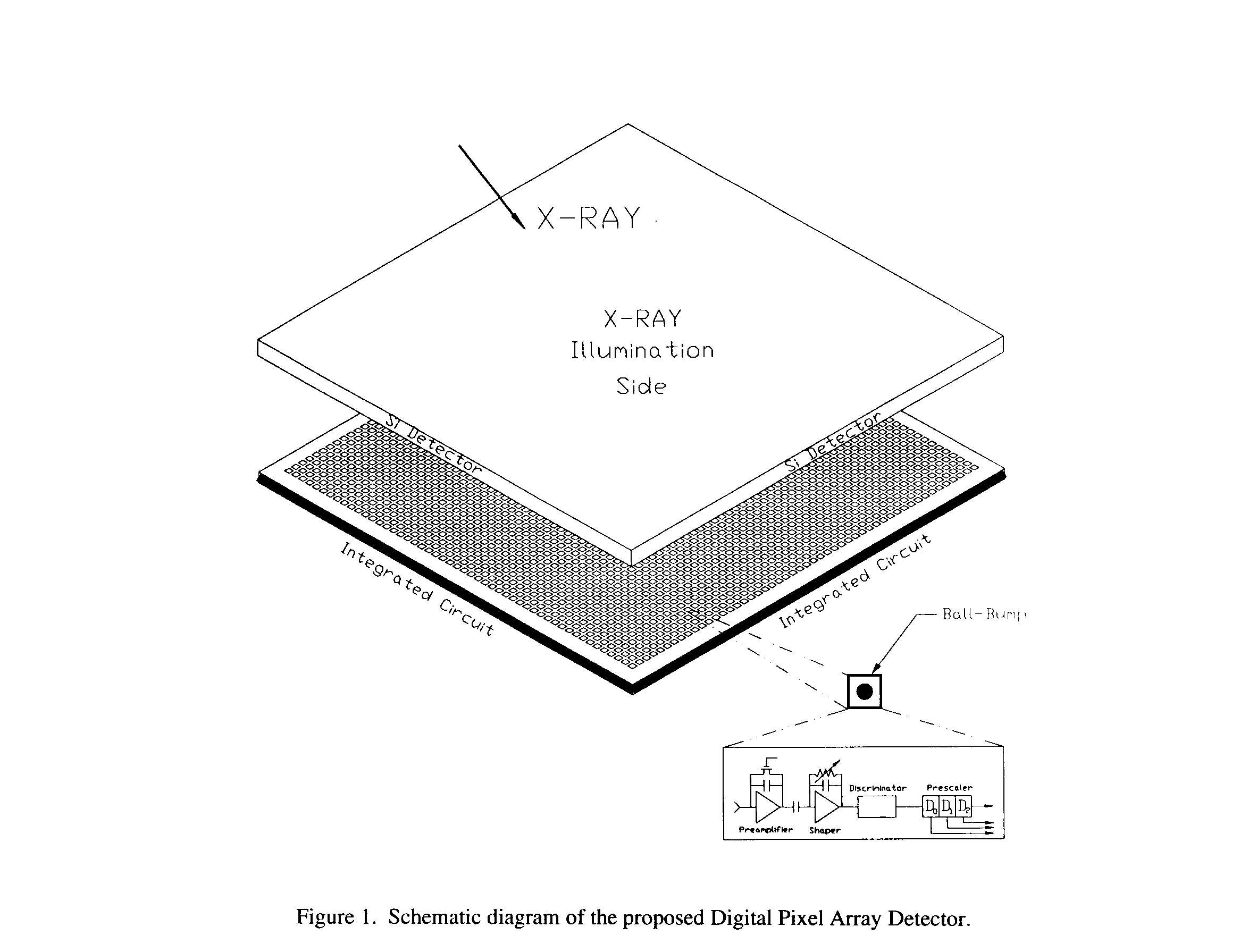
The Digital Pixel Array Detector (DPAD) presently being designed in our laboratory (2) will offer a substantial (two or three orders of magnitude) improvement over present technology and, for the first time, offer truly frameless readout for high speed time resolved crystallography. The detector consists of a reverse-biased Si diode array bump-bonded to an Application Specific Integrated Circuit (ASIC) (Fig. 1). The detector pixel pitch is 150
mm and the charge collection electrode is 100 x 100 mm2.
The ASIC contains both analog and digital processing circuitry which process a photon hit and generates the associated pixel address in less than 80 ns. Each pixel processor has a preamplifier, shaper, differential discriminator and a 3 bit pre-scaler which divides the pixel event rate by 8 to reduced band width requirements. An overflow bit or pseudo 4 bit starts the readout logic sequence to generate the pixel address. The event-driven address is generated by the column architecture (3). The column architecture was designed at Lawrence Berkeley National Laboratory for the high energy physics pixel detector to meet the demand of charge particle tracking at high luminosity particle accelerator beams. It is very well suited for this crystallographic application and many other biophysics applications. By optimizing the preams and shaper constants for photon counting, a maximum hit rate of 1 million photon/sec can be realized. For the targeted detector size of 1000 x 1000 pixels, average hit rates of up to 32 billion photon/sec for the whole detector can be achieved. In order to test the design of this new detector, we have built an 8 x 8 pixel array prototype.
3 The 8 x 8 Pixel Array Prototype Detector
The 8 x 8 prototype detector consists of a monolithic Si diode array that is bump-bonded to the ASIC readout with gold or Indium bumps and reversed biased to +100 V (typical). The 300
mm thick detector has a pixel pitch of 150 mm and a charge collection electrode of 100 x 100 mm2. Incident X-rays through direct photon conversion are absorbed in the Si where they create electron/hole pairs. For Si, 3.6 eV is needed on average to create one (e- -h pair) (ref xx). This measured charge pulse is then amplified, shaped (for noise optimization) and fed to a differential discriminator with an adjustable threshold, where the photon hit is converted to a digital address. Fig. 2 shows the detector and preams connected to the test-processing electronics. The present measurements have been target towards characterization of the front-end analog electronics, and the characterization of Si detector pixel geometry.The front-end analog electronics has been designed in the HP 0.8
mm 3 metal process and consists of a preamplifier with a DC reset and a shaping amplifier which forms a RC-(CR)2 shaping network. The combined gain of the circuit is 690 mV/fC or 110 mV/1000 e-, with a measured noise level of 60 e- (rms) at 5.9 keV (55Fe) using a Si detector with a total input capacitance 0.3 pF. The overall power consumption is 50 mW/channel. A complete description of the circuit can be found in Refs. (xx). Table 1 lists some of the more important circuit characteristics.Table 1. DPAD Analog Front-End Electronics Measured Values
Amplifier Parameters Measured Values
Total gain 110 mv/1000 e-
Reset time (adjustable) 1
msec.Shaping time 100 ns
(50 to 150 ns adjustable)
Power (analog only) 50
mW/channelNoise at 5.9 keV 60 e- rms
(Si pixel capacitance 0.3 pF) (480 eV)
4 Pixel Analog Readout
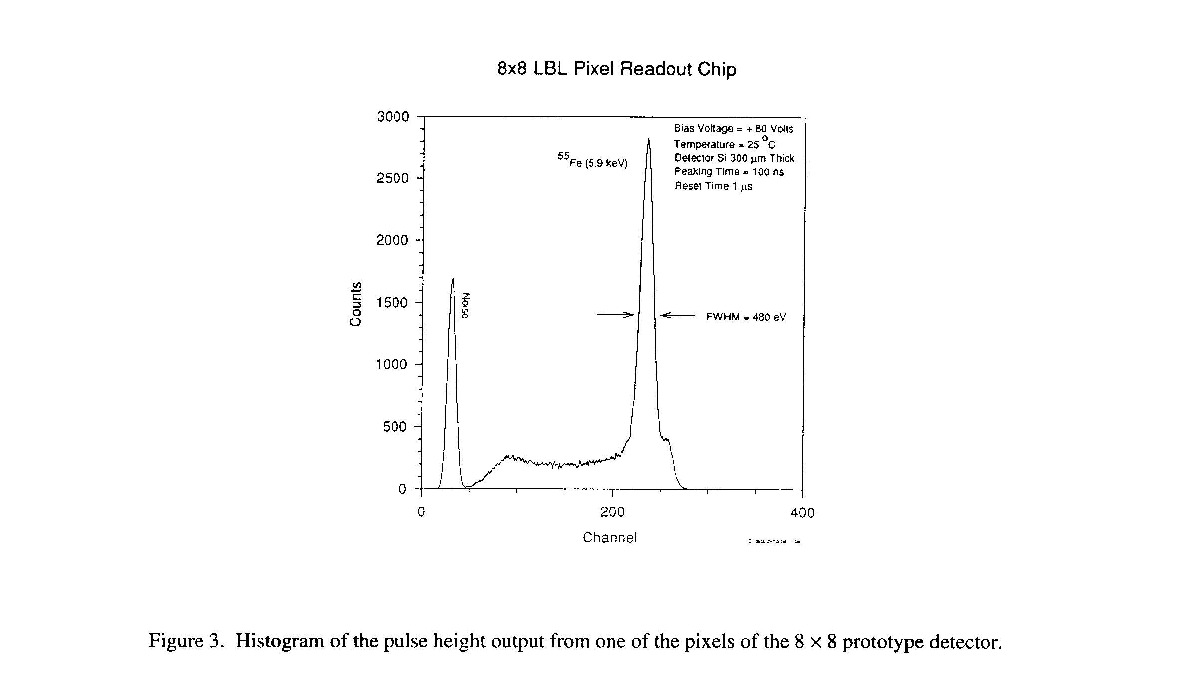
Figure 3 shows the histogram of the pulse height output from one of the pixels, when the prototype is irradiated with X-ray from an 55Fe source. The full width at half maximum (FWHM) at the 5.89 keV line is found to be 480 eV (rms -60 e-) and the 6.49 keV K
b line is visible a small hump just to the right of the 5.89 keV. The result is remarkable because the pixel array detector is working at room temperature. Until now, to achieve this kind of precision, a single detector must be cooled down to -30° C. The small plateau at lower energies to the left of the 5.89 keV peak is the result of charge trapping due to an oxide layer on the surface of the detector between the electrodes. Future detectors will be optimized to reduce this trapping effect.
5 Photon Counting
For crystallographic applications the detector must have a large dynamic range and a small point-spread function. This will allow the accurate and simultaneous recording of extremely strong and weak reflections separated by only a few hundred microns. Due to the short reset time of the preamplifier (< 1
ms), the dynamic range of the DPAD is only limited by the total number of scaler data bits, for pixel counting rates (£ 1 MHz).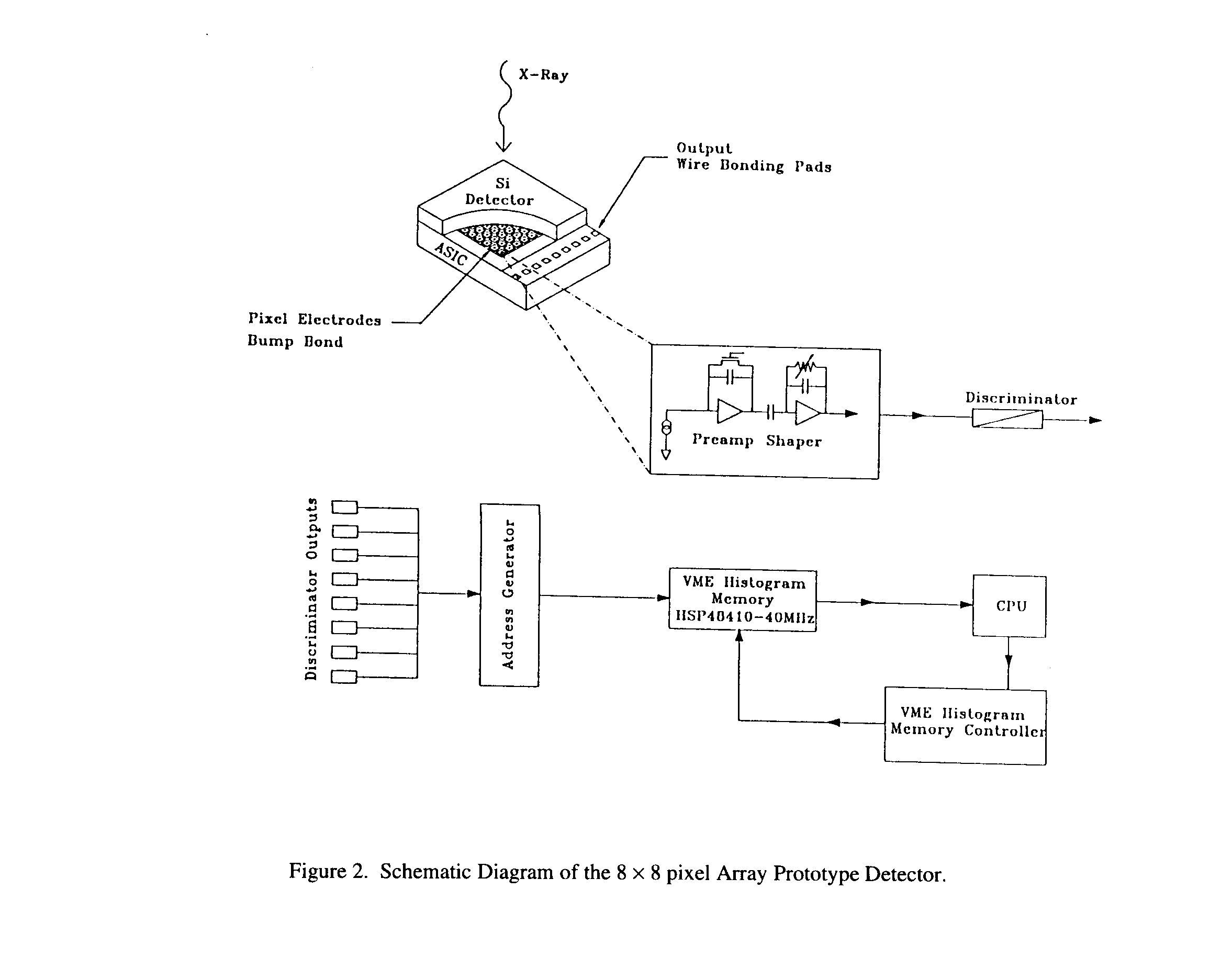
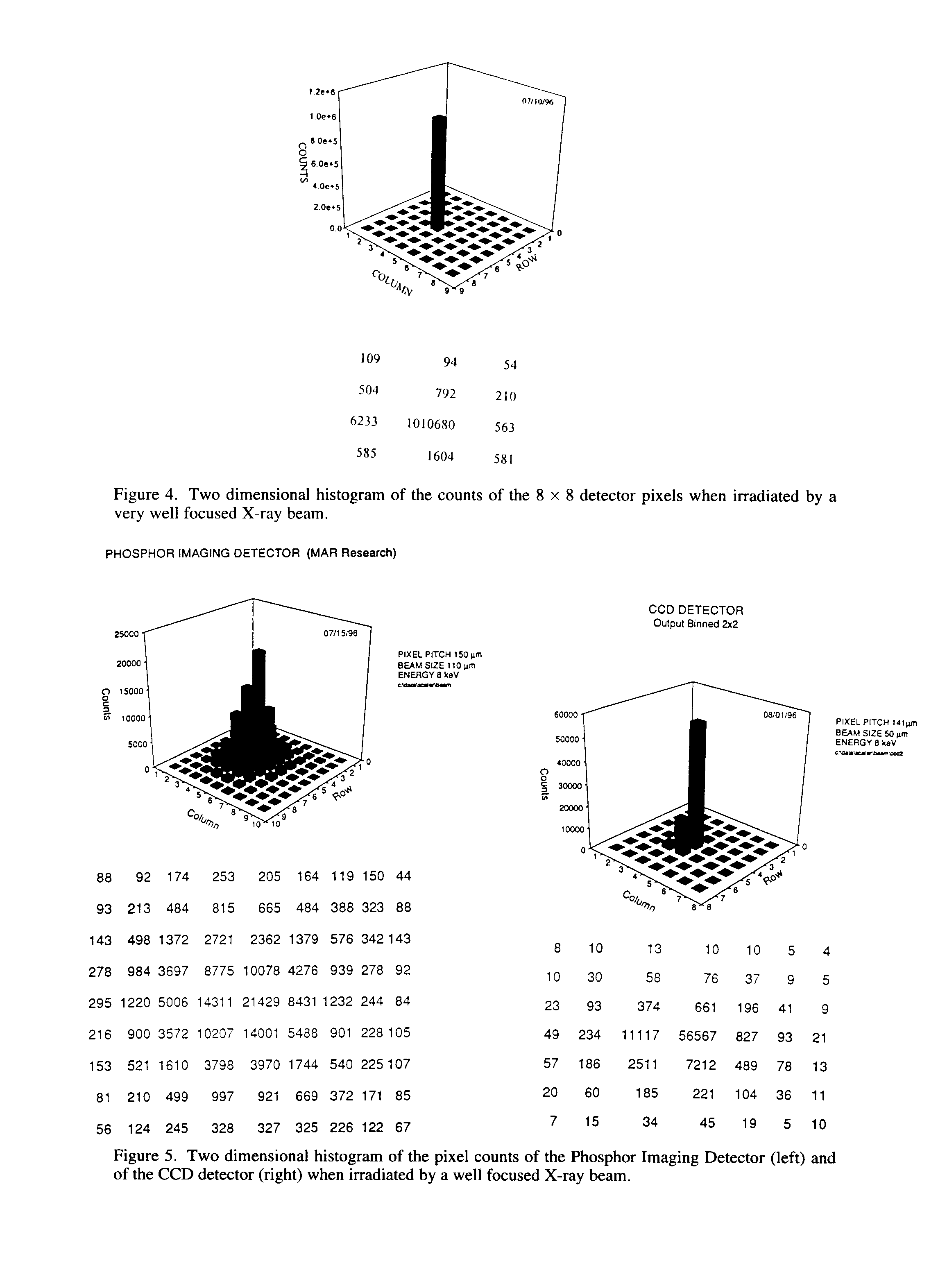
In order to measure the single pixel performance, a collimator was constructed using stacked tantalum foils in which a 35
mm hole has been laser drilled. The collimator was then attached to a gold rotating anode that is optimized for the Au La (9.7 keV) X-ray. Figure 4 shows a two-dimensional histogram of the X-ray counts of the detector pixels when placed at 5 mm from the collimator. From the plot it is observed that the signal-to-background is three decades at the acquisition time of 1000 s and a discriminator setting of 50 mV. This plot clearly shows the superiority of the new (DPAD) over the more conventional detectors for protein crystallography (phosphor imaging plates (4) and CCD (5) detectors) (See Fig. 5). The full-width at 1/100 maximum (G0.01) for the DPAD is less than 1 pixel width (150 mm). This value is increased to approximately 350 mm for the CCD and approaches 1000 mm for the imaging plate. Also, the DPAD can integrate digitally over long periods of time (in this case 1000s) without induced background noise due to dark current. As demonstrated here with digital integration, the DPAD has an almost infinite dynamic range, where both the imaging plate and the CCD detector (even when cooled to -50° C) are limited by saturation effects.
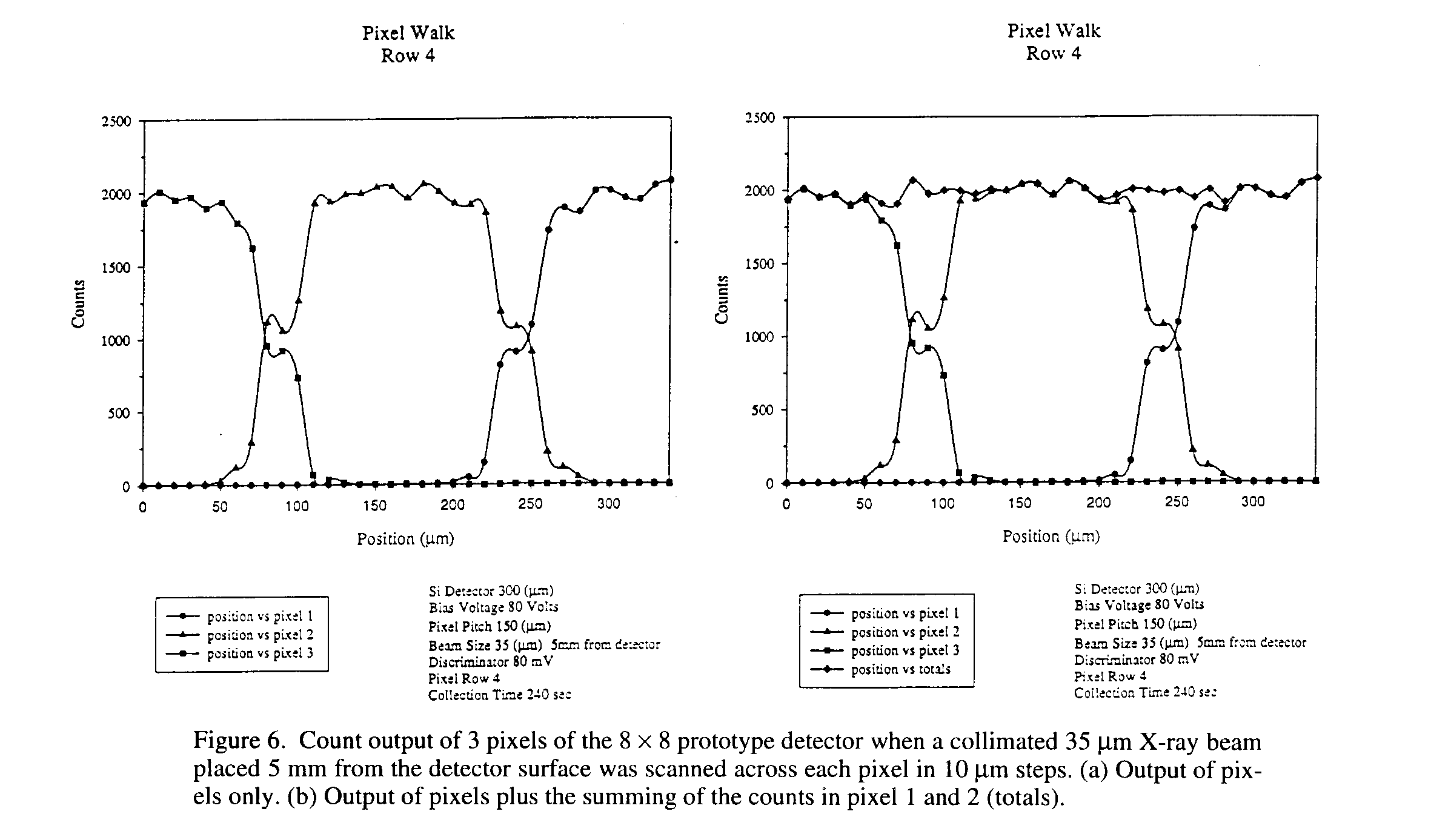
6 Pixel Walk
A study of the interstitial spacing was conducted to understand the point-spread function and charge sharing that may occur at the gap between neighboring pixels. Figure 6 shows a pixel walk plot of three pixels side by side. To make the measurement, a collimated 35 mm X-ray beam, placed 5 mm from the detector surface was scanned across each pixel in 10 mm steps. Counts from each pixel were then recorded. From the graph it can be seen that the raise (or fall) of the counting rate on the edge of a pixel could be simply due to the shape of the X-ray beam which should have a FWHM of about 35 mm. More importantly is that the plot shows the gaps between pixels behave in a similar manner and are quite symmetric. In addition, Plot A in Fig. 6 clearly shows that the pixel detector does not have an "dead" space. The charge is efficiently collected in all areas of the detector including the area between the charge collection electrodes (i.e. the 50 mm spacing). From plot B in Figure 6, the summing of the counts in pixels 1, 2 and 3 (totals) show little or no "double counts" at the pixel gap. From this, the point-spread function is observed to be near zero with the discriminator setting of 80 mV and a 10 mm step size. This is in agreement with typical diffusion length for this detector geometry which is found to be about 5 mm.
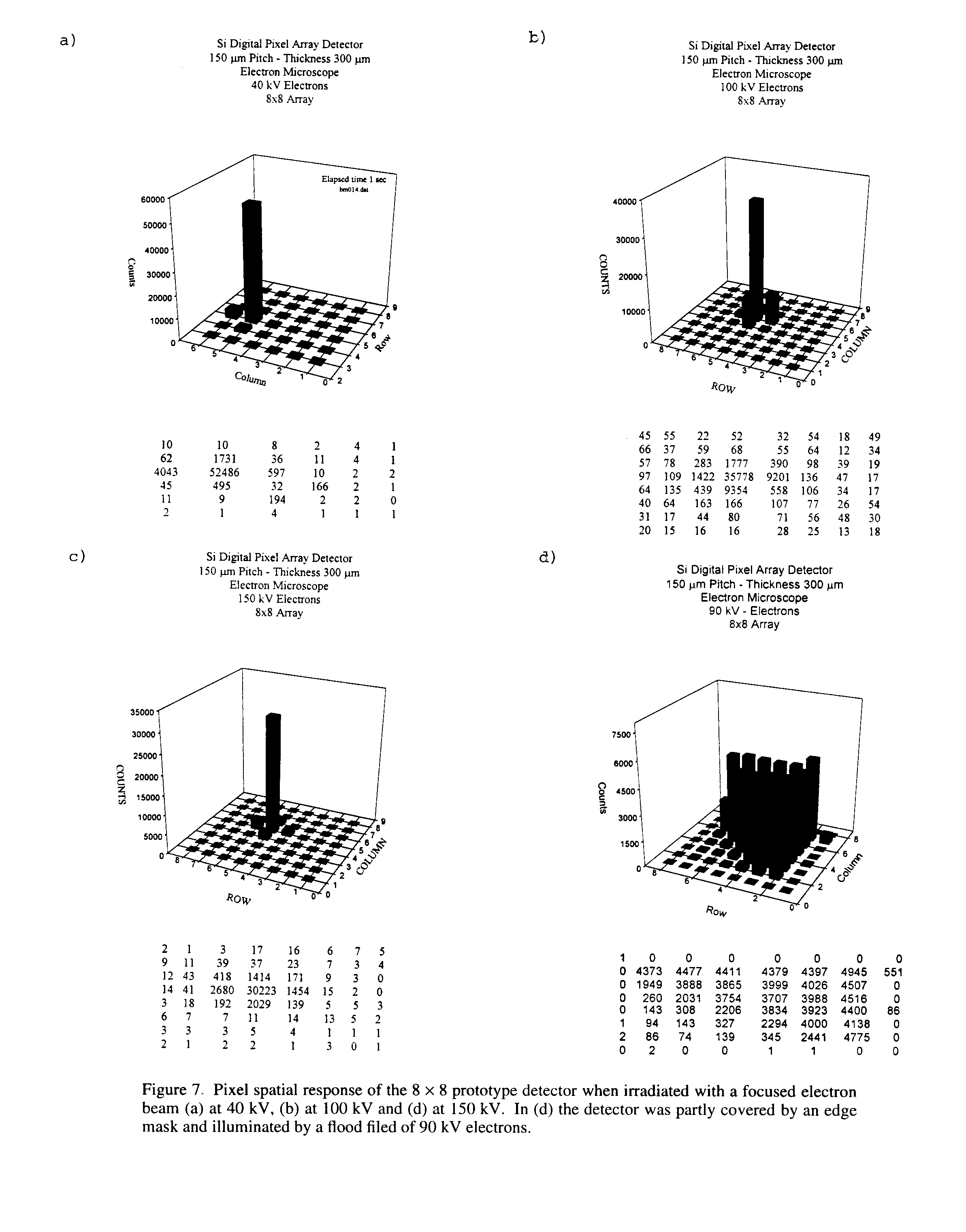
7 Application to Electron Microscopy
In order to test the feasibility of using this type of detection for electron microscopy, the prototype detector was put in a JEOL-2000 EX electron microscope in the voltage range of 20-200 kV. The detector was mounted on a special flange at the bottom of the electron microscope. Figures 7a-c show the pixel spatial response of the 2D detector when illuminated with a focused electron beam at 40 kV, 100 kV and 150 kV. The counts are still very well localized especially with beam energy below 100 kV; above 100 kV the range of some incident electrons in silicon could be above the pitch of the pixel (150 micron).
Figure 7d shows the response of the detector when it was partly covered by an edge mask and illuminated by a flood field of 90 kV electrons. The above results are extremely encouraging, especially if one considers that the preams designed for low energy X-rays (about 8 to 15 Kev) were saturated by electron of energy above 50 kV. There was no collimator, the electrons were simply focused but with some straying.
In the future, with better designed pream and with a clever interpolation of the pulse height output of all the pixels hit by one incident electron, the spatial resolution of the Digital Pixel Array Detector for Electron Microscopy could be as good as 50 mm. This kind of detector will allow the determination of 3D structure of macromolecules from single particles electron micrographs, i.e. it will eliminate the need to get large and well diffracted crystals which have been proving to be extremely difficult for some macromolecules (6).
8 Conclusion
First results of the 8 x 8 Si pixel detector are very encouraging. The results demonstrate that a low-noise pixel array can be constructed and operated at room temperature. The detector analog electronics is capable of processing charge pulses at the designed hit rate greater than 1 x 10⁶ photons/s with an energy resolution of 480 eV (FWHM) at room temperature. Also, the Si pixel detector displayed quite uniform digital behavior. With the low points-pread function it can provide excellent digital information at a 150 mm pitch and with the increasing availability of fine line CMOS technology, pixel sizes less than 100 mm may be feasible soon. A 16 x 16 prototype ASIC is presently being tested which include the compute column architecture. Early results are very promising and have already demonstrated the complete architecture functionality with no loss in the projected photon counting dynamic range. Once the ASIC has been fully characterized a detector hybrid will be made and tested.
Hopefully in a year, a modular 50 x 50 pixel array detector will be designed and checked out. We will then plan to assemble 400 of these modular detectors to form a 1000 x 1000 pixel array detector.
In a standard monochromatic protein crystallography experiment, this new detector could reduce the data collection time of a whole set of data from many hours to 45 seconds or less. This reduction is very important for very large macromolecule complexes (like Ribosome) whose crystals can suffer rapid decay in the X-ray beam.
In Laue diffraction, using a whole band of X-rays with wavelengths from 0.5 to 2.5 A, this new detector will allow the possibility to study transient phenomena in crystals using time-resolved experiments. With its ability for precise timing, zero readout time, and enough storage for up to 16 successive pictures, the Digital Pixel Array Detector (DPAD) is ideally suited for this kind of experiment. With the ability to detect Up to 106 photon/sec, the DPAD detector will allow a time interval of 10 msec per picture.
As we have seen above, the DPAD detector could one day be very useful also in electron microscopy. It is interesting to notice, that all the techniques underlying the making of the DPAD detector (CMOS, High Density Interconnection, etc.) are still evolving rapidly, allowing a many-fold improvement in a few years. Therefore, it is not exaggerated to call this detector a detector for the year 2000 and beyond.
References
1. Moffat, K. (1989) Time-Resolved Macromolecular Crystallography, Ann. Rev. Biophys. Biophys. Chem. 18, 309-332.
2. Beuville, E., Cork, C., Earnest, T., Mar, W., Millaud, J., Nygren, D., Padmore, H., Turko, B., Zizka, G., Datte, P., and Xuong, N.-H. (1996) A 2D Smart Pixel Detector for Time Resolved Protein Crystallography, IEEE Trans. on NucL Sci. 43, 1243-1247. Xuong, N.-H. (1996) Challenges in Macromolecules Structural Determination, Proc. VACETS VTIC'96, pgs. 1-08-16; VACETS, PO Box 4168, McLean, VA 22103-4168 USA.
3. Millaud, J., and Nygren, D. (1996) IEEE Trans. Nucl. Sci. NS 43(3), 1243.
4. Sato, M., Yamamota, M., Imada, K., Katsube, Y., et al. (1992) A High-Speed Data-Collection System for Large-Unit-Cell Crystals Using an Imaging Plate as a Detector, J. Appl. Cryst. 25, 348-357.
5. O'Mara et al. (1993) Modular CCD Camera Development for X-ray Crystallography, Proc. SPIE 1656, 450-456.
6. Bottcher, B., Wynne, S.A., and Growther, R.A. (1997) Determination of the Fold of the Core Protein of Hepatitis B Virus by Electron Microscope, Nature 386, 88-91.